Hafnia’s Hidden Switch: What Intrinsic Antiferroelectricity Could Change in Electronics
A Science study argues that hafnium oxide is intrinsically antiferroelectric down to a 0.6-nanometer film. The result does not make a new memory chip overnight, but it gives engineers a familiar, silicon-compatible material with a clearer electrical identity to work from.

A material already used inside modern electronics has acquired a more precise scientific identity. In a paper published in Science, researchers from the University of Nebraska–Lincoln report evidence that hafnium oxide, or hafnia, is intrinsically antiferroelectric. They observed the defining behavior in extremely thin films, with the effect persisting down to about 0.6 nanometers—roughly a few atomic layers—and remaining stable at temperatures as high as 850 °C.
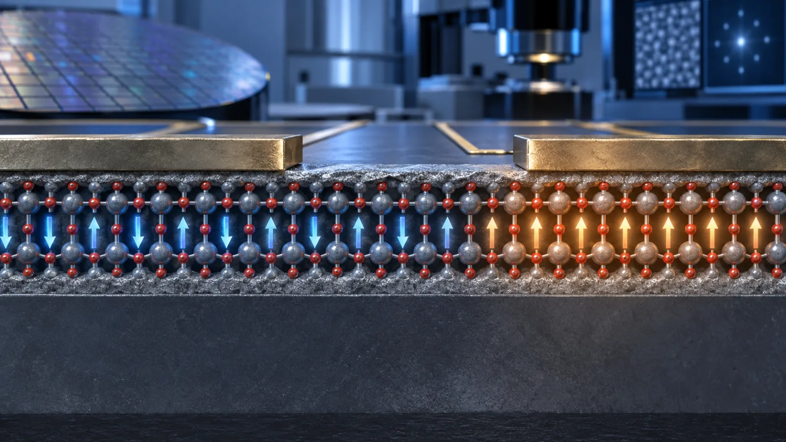
That is a meaningful result in materials science because hafnia is not an exotic crystal that would first need an industrial supply chain. It is a hard, heat-resistant oxide already familiar to semiconductor manufacturing. The study therefore connects a newly clarified property to an established material platform. The practical opportunity is real, but it is still an opportunity: no commercial processor, capacitor or cooling device follows automatically from this experiment.
The most useful way to read the finding is as a change in the starting conditions for engineering. For years, researchers have seen antiferroelectric-like electrical curves in hafnia films while debating whether those curves represented a genuine property of the material or an effect caused by defects, trapped charge, interfaces or processing history. The new work brings structural evidence, electrical measurements, microscopy and theory together in support of intrinsic antiferroelectricity.
What the researchers actually showed
The study, titled Antiferroelectric hafnia down to the 2D limit, was led by Xiaoshan Xu, Alexei Gruverman and Evgeny Tsymbal, with contributions from collaborators including Rohan Mishra of Washington University in St. Louis. The researchers grew very thin hafnium-oxide films using pulsed-laser deposition. An underlying crystal placed the film under compression and helped stabilize the atomic arrangement associated with the antiferroelectric state.
The word stabilize matters here. A material’s chemical formula does not determine every useful electronic property by itself. The same compound can behave differently when its atoms adopt different crystal structures, when strain changes the distances between them, or when surfaces and interfaces become a large part of the sample. At nanometer thicknesses, those details are not side issues. They are the device.
The Nebraska team investigated hafnia films across a range of thicknesses and found that the antiferroelectric order did not fade as the film became thinner. According to the university’s account of the work, the order became more stable in the thinnest samples and remained observable to 0.6 nanometers. The film also retained its structure at temperatures up to 850 °C. That combination—atomic-scale thickness and high-temperature stability—is the part with the clearest engineering significance.
The researchers did not rely on a single electrical trace. The evidence included three features associated with a genuine antiferroelectric: a characteristic double hysteresis loop, antiparallel polar sublattices and boundaries between different structural phases. Scanning-probe measurements showed that the film could move between an antipolar state and a polar state. Atomic-scale imaging was used to examine the quality of the crystal, while theoretical calculations provided an independent check on whether the observed behavior fit the expected structure.
This combination is stronger than simply saying that a capacitor had an unusual curve. Electrical hysteresis can have several causes. Charge can become trapped, defects can move, and interfaces can create apparent switching. Establishing the microscopic arrangement that produces the response is what turns a suggestive measurement into a materials claim.
Antiferroelectricity in plain language
An antiferroelectric is related to a ferroelectric, but the internal arrangement is different. In a ferroelectric, microscopic electric dipoles can align so that the material has a net polarization. That polarization can often be reversed by applying an electric field, which makes ferroelectrics useful for nonvolatile memory, sensors and actuators.
In an antiferroelectric, neighboring dipoles tend to point in opposite directions. Their effects largely cancel when no external field is applied, leaving the material in an antipolar state. Apply a sufficiently strong field and the arrangement can switch into a polar state. Reduce the field, and the material can return toward its original configuration.
A simplified picture looks like this:
No applied field:       ↑ ↓ ↑ ↓   antipolar arrangement
Strong applied field:   ↑ ↑ ↑ ↑   polar arrangement
Field removed:          ↑ ↓ ↑ ↓   return toward antipolar state
The real crystal is more complicated than this diagram, and the transition depends on temperature, thickness, electrodes, frequency, defects and the strength of the applied field. Still, the diagram captures why engineers care. An antiferroelectric can absorb electrical energy during a field-induced transition and release it again. It can also provide a switchable internal state without requiring a permanent net polarization at rest.
The double hysteresis loop is the familiar electrical signature of that behavior. A normal dielectric responds to a field without switching between two long-lived polarization states. A ferroelectric usually produces a single hysteresis loop. An antiferroelectric can show two field thresholds: one for entering the polar state and another for returning to the antipolar state. Those thresholds are not merely a visual curiosity. They describe how much voltage is needed to move energy into and out of the material and how much energy is dissipated in the process.
Why hafnia is a useful material platform
Hafnium oxide has been important in semiconductor technology because it combines useful insulation with a high dielectric constant. It has also been studied in ferroelectric devices, where carefully controlled thin films can retain switchable polarization. The compound is compatible with silicon-based processing more readily than many unusual functional materials, and it can tolerate processing environments that would damage more delicate compounds.
That existing familiarity changes the development problem. If a new property appears in a material already deposited, patterned and integrated by chip manufacturers, researchers can investigate whether it fits existing process steps. They do not begin with the additional challenge of replacing the material, building a supply chain and inventing an entirely new fabrication method. Compatibility does not guarantee manufacturability, but it shortens the list of unknowns.
Hafnia also avoids one problem associated with several well-known antiferroelectrics: lead. Lead-based materials can deliver strong electromechanical or dielectric performance, but toxicity and environmental handling complicate their use at scale. A lead-free antiferroelectric that can be made extremely thin and integrated with silicon is therefore attractive even before anyone claims a specific product advantage.
The new result also addresses a long-running conceptual question. Scientists had observed antiferroelectric-like responses in hafnia, but some interpretations treated the response as extrinsic. In that view, the apparent switching might come from charge redistribution, oxygen vacancies or interfaces rather than a stable antiferroelectric phase in the bulk of the film. The Nebraska study argues that high-quality monocrystalline hafnia exhibits the behavior intrinsically.
That distinction matters for design. If the effect is intrinsic, engineers can try to control it through crystal orientation, strain, thickness, electrodes and temperature with a clearer physical model. If it exists only because of an accidental collection of defects, improving the material might remove the effect rather than strengthen it.
The first possible application: smaller, fast energy-storage components
The most direct application area is the capacitor. Capacitors store electrical energy in an electric field, and they are present throughout power electronics, communications equipment, sensors and processors. Their size, voltage rating, leakage, speed and reliability all influence the design of a system.
Antiferroelectric hafnia is interesting because a field-induced phase transition can support high recoverable energy density in a very small volume. Hafnia’s high breakdown strength and thin-film compatibility add to that attraction. The material could eventually help create compact capacitors for local voltage regulation, power delivery or transient energy storage near electronic circuits.
The word eventually carries most of the qualification. The reported study establishes a microscopic property in carefully prepared films. It does not demonstrate a packaged capacitor operating for billions of switching cycles, under production conditions, with a competitive energy density and acceptable efficiency. Those are separate engineering tests.
Capacitor developers will need to measure several practical quantities:
- How much energy can be recovered rather than lost as heat during each cycle?
- How does the response change when the film is deposited on a standard silicon wafer instead of a specially chosen substrate?
- Can the material be made uniformly across a large wafer?
- What voltage is required once real electrodes and insulating layers are included?
- Does repeated cycling cause fatigue, leakage or a permanent shift in the switching thresholds?
- How sensitive is the result to oxygen vacancies, grain boundaries and surface contamination?
The university’s energy-research program identifies many of these issues as open development targets, including phase stability, leakage current, retention, processing conditions, electrode choice and performance across temperature, frequency and field strength. That is a useful reminder that a promising phase is not the same thing as a finished energy-storage component.
Memory is possible, but the route is not automatic
The same switchability makes antiferroelectrics relevant to memory research. Electronic memory requires a physical state that can be written, read and retained with low error. A material that changes polarization under voltage can, in principle, influence a transistor, capacitor or tunnel junction and represent information in a compact area.
Hafnia has already attracted attention in ferroelectric memory because it can be made thin and can be integrated with semiconductor processes. Intrinsic antiferroelectricity adds another design option. Engineers might use the transition between antipolar and polar states, exploit its field thresholds, or combine antiferroelectric and ferroelectric regions in a device with several electrical states.
But memory has a demanding definition of success. A laboratory sample can switch once and still be useless as memory. A practical device must switch predictably across a large array, retain information for a specified period, survive repeated writes, tolerate temperature variation and remain readable after neighboring cells are operated. It also must fit within the voltage and thermal budget of the surrounding circuitry.
There is a further issue at ultrathin dimensions. Thin films reduce the volume needed for each cell, but they also make interfaces and defects proportionally more influential. A 0.6-nanometer film may be an excellent demonstration of a stable physical state and a difficult manufacturing target at the same time. A production line must control thickness, composition and uniformity over millions or billions of devices, not only produce an exceptional crystal in a research chamber.
For that reason, the sensible near-term outcome is not a prediction that hafnia will replace flash memory or become the next universal chip material. The nearer outcome is a better map of the design space. Researchers now have evidence that the antiferroelectric state can survive at a thickness where conventional intuition might expect it to disappear. That gives device teams a reason to test architectures that previously looked too fragile or too dependent on defects.
Could it help with solid-state cooling?
Antiferroelectrics are also studied for electrocaloric cooling. In an electrocaloric material, changing an electric field changes the arrangement of dipoles and therefore the material’s entropy and temperature. A carefully designed device can use that effect to move heat without the refrigerant gases used in conventional vapor-compression systems.
Hafnia’s possible advantage would be its thin-film form, which could make it easier to build compact cooling elements and integrate them close to heat-producing electronics. A cooling layer placed near a sensor, laser, memory array or power-management component could be useful if it delivered enough temperature change with acceptable voltage and efficiency. The high-temperature stability reported in the study is also relevant to harsh environments, though it should not be confused with a demonstrated cooling cycle.
The cooling case is especially dependent on measurements that are not supplied by the headline result. Researchers would need to establish the electrocaloric temperature change, heat capacity, thermal conductivity, response speed, hysteresis loss and lifetime under repeated operation. A material can have an attractive field-induced transition and still be a poor refrigerator if most of the input energy becomes irreversible heat.
There is also a system question. The cooling element must transfer heat to a sink, and the electrodes, substrate and packaging can dominate the thermal behavior. A promising nanoscale effect only becomes useful when it is embedded in a complete thermal design.
Why the two-dimensional limit is important
The phrase “2D limit” can sound like a claim that a material is literally a single mathematical plane. In experimental materials science, it generally refers to behavior that survives as the thickness approaches the two-dimensional regime, where only a few atomic layers remain.
Many properties become harder to maintain at that scale. Surface energy grows in importance, atoms have fewer neighbors, and the interface with a substrate can overwhelm the behavior of the film. Ferroelectric and antiferroelectric ordering are particularly sensitive because they depend on coordinated displacements across a lattice. If the ordering disappears below a critical thickness, it cannot be used in the smallest devices.
The Nebraska results go in the opposite direction for the samples studied: the antiferroelectric structure became more stable as the film was thinned, rather than simply collapsing. That result challenges a common expectation and may help explain why hafnia has been so productive in nanoscale electronics. It also highlights the role of strain. The substrate did not merely hold the film in place; it helped create the conditions under which the desired atomic arrangement became favorable.
This is the kind of result that can influence several research fields at once. Device engineers see a possible ultrathin dielectric. Materials theorists gain a clean system for studying competing polar and antipolar phases. Semiconductor researchers gain a candidate compatible with existing processing. Energy-storage researchers gain a lead-free platform whose field-induced transition can be tuned. None of these fields has a finished product yet, but all have a more concrete material to investigate.
What remains uncertain
The paper is a strong materials result, not a product qualification. The main uncertainties are practical and substantial.
First, the films were grown under controlled laboratory conditions on a substrate selected to stabilize the structure. Industrial devices may use different substrates, seed layers, electrodes and thermal budgets. The same ordering may be harder to produce when the film must be deposited quickly and uniformly across a large wafer.
Second, the reported high-temperature stability describes the material structure under the study’s conditions. It does not establish how a complete device behaves at 850 °C, nor does it mean that a phone, computer or memory module could operate at that temperature. Semiconductor devices contain many materials, and the least heat-tolerant component usually sets the system limit.
Third, the useful electrical performance has to be benchmarked against established dielectrics and antiferroelectric systems. Energy density alone is not enough. A capacitor must also have low loss, low leakage, high endurance, a controllable voltage window and predictable behavior across manufacturing variation. A memory cell must meet retention and error targets. A cooler must move heat efficiently.
Fourth, the study clarifies the intrinsic property but does not eliminate the influence of imperfections. Real films will contain interfaces, vacancies, roughness and perhaps multiple crystal phases. Those features may help or hurt the switching response. Understanding them will be part of the engineering work rather than a footnote to it.
Finally, the timeline is unknown. Basic materials discoveries can move quickly when they fit an existing industrial process, but they can also remain in research laboratories for years if reliability or integration problems appear. The reasonable claim today is that hafnia has become a more credible platform for antiferroelectric devices—not that those devices are ready for mass production.
Why this counts as useful technology news
Good technology news is not limited to a new product launch. Sometimes the important improvement is that researchers have removed ambiguity from a material already sitting near the center of an industry. That is what makes this study valuable.
Hafnium oxide was already useful. The new work does not grant it a magical ability or promise a sudden transformation of computing. It provides evidence that a rare and potentially valuable electrical behavior belongs to the material itself, survives at astonishingly small thicknesses and can be studied on a platform compatible with silicon electronics. It replaces a disputed interpretation with a more coherent physical picture.
That change can influence what engineers choose to build and what measurements they consider worth making. It may lead to better thin-film capacitors, denser memory concepts, compact electrocaloric coolers or entirely different devices that depend on field-controlled phase transitions. The benefits, if they arrive, will come through the unglamorous stages: wafer-scale deposition, reliability testing, modeling, packaging and comparison with products that already work.
For now, the strongest conclusion is modest and specific. Hafnia is not merely imitating antiferroelectric behavior because a defect happens to trap charge. Under the right structural conditions, it appears to be an intrinsic antiferroelectric, even when reduced to the thickness range demanded by modern nanoscale electronics. That is a firm new foundation for the next round of experiments—and a better reason for optimism than a promise of an instant breakthrough.
Comments
Sign in to comment.
No comments yet.